PANELMAP
PANELMAP – Metrology Analysis Software for Panels and Solar Cells
PANELMAP is a specialized software solution for the evaluation and visualization of spatially resolved measurement data on rectangular substrates, including flat panels, semiconductor panels, and solar cells. The software is designed for engineers who require reliable, tool-independent analysis of metrology data in both development and production environments.
PANELMAP supports the import and analysis of measurement data from a wide range of metrology systems, including ellipsometers, thin-film thickness measurement tools, four-point probe systems, optical characterization equipment, and I-V characterization systems. In addition, it integrates data from advanced geometry gauges for thickness and resistivity measurements on substrates up to 300 mm, as well as optical metrology systems such as interferometers used for precise layer thickness evaluation. Both ASCII and instrument-specific data formats can be processed, allowing straightforward integration into existing workflows without dependence on a particular hardware vendor.
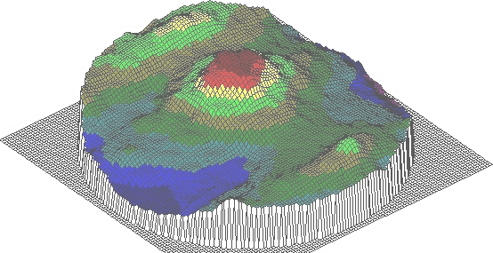
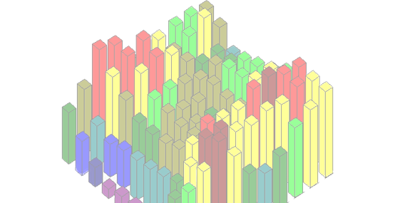
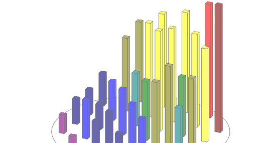
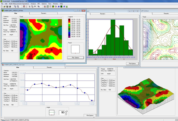
The software provides comprehensive visualization capabilities, including two-dimensional maps, multicolor contour plots, three-dimensional surface and wireframe representations, line scans, and statistical histograms. These visualization tools allow engineers to quickly identify spatial inhomogeneities, edge effects, gradients, and systematic process deviations across panels or solar cells.
In addition to visualization, PANELMAP offers powerful data processing functions. Measurement maps can be mathematically combined through arithmetic operations such as addition, subtraction, or division. Derivative calculations, sigma filtering, and statistical evaluations support detailed process analysis and outlier detection. Multiple datasets can be directly compared, enabling efficient difference mapping and benchmarking of production runs or equipment performance.
Transformation features such as rotation, mirroring, coordinate shifting, interpolation of measurement grids, and dataset merging ensure accurate alignment and consistent comparison of results from different tools or process steps.
By enabling structured offline analysis, PANELMAP supports faster root-cause identification, improved process understanding, and enhanced spatial uniformity control in both R&D and high-volume manufacturing of panels and solar cells.
You May Also Be Interested In
Check Out Wafermap – Advanced Software for Semiconductor Wafer Metrology and Spatial Data Visualization.
Discover Wafer Mapping Application Notes – Semiconductor Metrology Analysis, Wafer Map Comparison, Contour Visualization, and SPC Integration.